
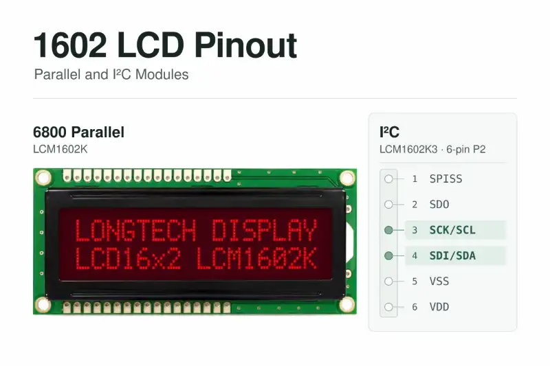
The parallel LCM1602K connects through a 16-pin 6800 header. On the LCM1602K3 in I²C mode, connect SCL, SDA, ground, and the 5 V supply to P2 pins 3, 4, 5, and 6, respectively. The tables below give the complete pin assignments for both versions.
A 1602 LCD display has 16 characters per row and two rows. We compare two of our COB character LCD modules with the same 80 × 36 mm outline. The shared outline makes this a practical example for an OEM that wants to keep the enclosure while choosing a host interface.
1602 LCD Pinout at a Glance
This guide covers the 5 V parallel version of the LCM1602K and the 5 V LCM1602K3 configured for I²C. On a COB module, the display controller is mounted on the PCB. When selecting a part, check the interface option and connector drawing for the version you will order.
| What to check | LCM1602K | LCM1602K3 |
| Display type | 16×2 COB character LCD | 16×2 COB character LCD |
| Module outline | 80 × 36 mm | 80 × 36 mm |
| Host interface | 6800 parallel, 4-bit or 8-bit | On-board I²C interface |
| Module connector | 16-pin header | Six-pin P2 header |
| Host signals | Six GPIO outputs in 4-bit write-only mode | SCL and SDA |
| Nominal module supply | 5 V at pin 2, ground at pin 1 | 5 V at P2 pin 6, ground at P2 pin 5 |
If your equipment already uses a parallel LCD and the board and cable are staying in service, compare the LCM1602K against the old pinout, logic levels, and initialization. If you are redesigning the host around an I²C bus, check the K3’s connector and serial protocol before finalizing the harness and firmware.
Finding Pin 1 on a 1602 LCD
Use the connector marking and the drawing view together. A printed 1 or a square pad can help identify the first pin. When inspecting the back of the PCB, compare it with the drawing’s stated viewing side before numbering the cable or PCB footprint.
LCM1602K 16-Pin Parallel LCD Pinout
The host uses RS to select an instruction or display data. It sets the data lines and pulses E to make a transfer. The R/W pin determines the transfer direction, so a design that only writes to the display can tie R/W low.
| Pin | Signal | Function |
| 1 | VSS | Module ground |
| 2 | VDD | Logic supply, nominally 5 V for this version |
| 3 | V0 | LCD contrast adjustment input |
| 4 | RS | Register select. Low selects instructions or status and high selects display data. |
| 5 | R/W | Read or write select. Low for write and high for read. |
| 6 | E | Parallel transfer enable |
| 7 | DB0 | Data bit 0, used in 8-bit mode |
| 8 | DB1 | Data bit 1, used in 8-bit mode |
| 9 | DB2 | Data bit 2, used in 8-bit mode |
| 10 | DB3 | Data bit 3, used in 8-bit mode |
| 11 | DB4 | Data bit 4, used in 4-bit and 8-bit modes |
| 12 | DB5 | Data bit 5, used in 4-bit and 8-bit modes |
| 13 | DB6 | Data bit 6, used in 4-bit and 8-bit modes |
| 14 | DB7 | Data bit 7, used in 4-bit and 8-bit modes |
| 15 | LED+ | LED backlight anode |
| 16 | LED− | LED backlight cathode |
Choosing 4-Bit or 8-Bit Wiring
For a 4-bit write-only connection, route the MCU outputs to RS, E, and DB4 through DB7. These are pins 4, 6, and 11–14. Tie pin 5, R/W, to VSS. The module drawing leaves DB0 through DB3 unused in this mode. After the firmware initializes the controller for 4-bit operation, it sends each byte in two transfers, high nibble first.
In 8-bit mode, connect DB0 through DB7 so the host can send one byte per enable cycle. If the firmware reads the busy flag, make R/W controllable and put the MCU data pins in input mode for the read. For write-only operation, observe the specified execution delay for each instruction. Clear Display and Return Home take longer than most other commands.
After initialization permits busy-flag reads, complete both enable cycles when reading the busy flag in 4-bit mode. The flag is on DB7 during the first transfer. The second transfer completes the read and keeps the next command aligned.
We commonly use the Sitronix ST7066U in our character LCD modules, and our catalog lists it for the LCM1602K family. The ST7066U and Hitachi HD44780U share basic parallel commands, including Clear Display (0x01) and Set DDRAM Address for positioning the cursor. Longtech character LCD catalog · Hitachi HD44780U datasheet
Use the timing and initialization sequence for the controller fitted to your module. In Sitronix’s 5 V 4-bit example, the host waits more than 40 ms after the controller supply exceeds 4.5 V before sending the first Function Set. Follow the complete startup sequence and the bus timing for the ST7066U version. Sitronix ST7066U datasheet
Setting Contrast and Wiring the Backlight
Pin 3, V0, sets the contrast. The module drawing expresses the LCD drive voltage as VDD − V0. One circuit connects a potentiometer between VDD and VSS and routes the wiper to V0. A drawing that specifies external bias uses the indicated bias rail instead. Adjust contrast while sending a test message and check it under your equipment’s operating conditions.
Pins 15 and 16 feed the LED backlight. Verify its voltage, current, and current-limiting arrangement for the ordered version. Check the voltage at pin 2 separately during bring-up. A lit backlight tells you that the LED circuit has power.
LCM1602K3 I²C LCD Pinout
The LCM1602K3 places a serial interface between the host and the LCD controller. The host talks to that interface over I²C. Locate the six-pin header marked P2 on the drawing. The board also has a separate P1 header.
| P2 pin | Drawing label | Function |
| 1 | SPISS | SPI chip select |
| 2 | SDO | SPI serial data output |
| 3 | SCK/SCL | I²C clock, connect to the host’s SCL |
| 4 | SDI/SDA | I²C data, connect to the host’s SDA |
| 5 | VSS | Ground, shared with the host and module supply |
| 6 | VDD | Nominal 5 V module supply |
Configuring the I²C Interface
Check the board instructions for selecting I²C mode and handling the SPI pins. Verify the address, supported clock rate, and pull-up arrangement for the supplied revision. On a shared bus, confirm the display’s address is available and that the bus speed suits the devices attached to it.
Check how the address is written in the communication manual. If it gives an 8-bit address byte including the read/write bit, shift that byte right by one for a driver that expects a 7-bit address. When possible, connect the display as the only target during the initial bench test. An acknowledgement confirms a response at that address. Send a short message using the module’s documented command format to verify that it can write characters. NXP I²C-bus specification
Connecting a 3.3 V MCU to a 5 V 1602 LCD
The 5 V rating in the pinout tables refers to module power. For a 3.3 V MCU, check the digital signals separately. Use the module and MCU electrical specifications at the supply voltages and loads in your design.
- Parallel signals. Compare the MCU’s minimum output-high voltage with the LCD’s minimum input-high threshold. Check that the MCU’s maximum output-low voltage meets the LCD’s input-low limit. If you read from the display, also verify the LCD output levels and the maximum voltage allowed at the MCU pins.
- I²C signals. Find the pull-ups on SDA and SCL and trace them to their rail. Each pin must tolerate the resulting idle-high voltage and recognize it as a valid high. If the host and module need separate voltage domains, use a suitable bidirectional I²C level shifter with pull-ups for each side.
The production harness affects the I²C waveform. Include any pull-ups already installed on the host or module when checking the effective resistance. At P2, measure the low level and rise time with the production harness connected and the bus running at the intended speed. NXP guidance on I²C pull-ups and rise time
1602 LCD Replacement Checklist
We check four areas before recommending a sample for an existing product. A complete part number and a drawing are especially helpful when the old screen came from a different supplier.
| Check | What to verify before ordering a sample |
| Mechanical fit | Mounting holes, viewing window, thickness, connector location, and cable clearance |
| Electrical fit | Pin 1 orientation, pin order, supply voltage, logic levels, and the backlight circuit |
| Firmware | Parallel bus width, initialization and timing, or I²C address, mode and command format |
| Installed display | Readability, character set, and startup behavior through the original enclosure window |
On older equipment with incomplete records, trace the harness and check continuity with power off. For a parallel display, check which data lines are wired and whether R/W is tied low. Capture E and the data lines at power-up if you need to confirm the bus mode. Use that information to choose a sample and test it with the production board and harness.
Once a sample passes, record the approved part number, connector drawing, and controller or serial configuration with the purchasing specification. That gives engineering and procurement a reference when the production order is placed.
Troubleshooting a Blank 1602 LCD Display
Measure at the display connector so a harness fault shows up in the test. Start with VDD relative to VSS at the module. Then check the control signals or I²C transactions while the host initializes the display.
| Symptom | First checks |
| Backlight is on and the display is blank | Verify module power at VDD and VSS. On the LCM1602K, check the V0 setting and the initialization sequence. |
| A row of blocks appears on the parallel LCD | Check contrast, then inspect RS, E, and the data lines during startup. Verify the wiring and initialization match the selected bus width. |
| The I²C address gets no acknowledgement | Verify P2 pin numbering, common ground, I²C mode, bus idle levels, and the address format used by the host. |
| The I²C address is acknowledged but the screen is blank | Confirm the responding device is the display. Send a documented display command and test message using the K3 command format. |
Once text appears, power-cycle the equipment and write to the first and last positions on both rows. In the ST7066U 16×2 example, the first and second rows start at DDRAM addresses 0x00 and 0x40. For a serial module, use its cursor-position command. Sitronix ST7066U display memory map
Use the strings the operator will see, including any degree symbols or custom alarm characters. Character ROM options can map the same byte to different glyphs, so a test with plain letters and numbers covers only part of the display check. Check the installed display from the intended viewing angle with the production backlight setting.
Using a PCF8574 I²C Backpack
A PCF8574 backpack uses an I/O expander to drive the parallel signals of an LCD. Its firmware library writes port bits that correspond to the adapter’s pin mapping. The LCM1602K3 receives serial commands through its own interface. Choose a driver that implements the command format for the module or adapter you are using. PCF8574 reference · Longtech Arduino LCD wiring guide
Request a 1602 LCD Pinout or Replacement
Send us the original model number and datasheet, or clear photos of the front, back, and connector. Include the host interface, supply voltage, and any mounting or backlight requirements. If you need to keep the PCB, cable, or firmware, tell us which of those are fixed. We can compare the pinout and drawing before you order an evaluation sample. Contact Longtech
